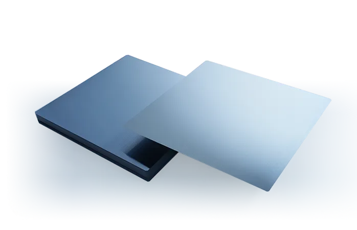
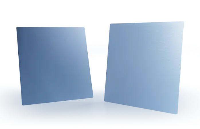
Wafer
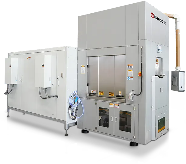
It is difficult to control yield of large thin stacked photovoltaic silicon wafers. We have been engaged in cutting for many years, continuously promoting thin wire, improving yield and performance of wafers. We focus on improving wire marks and TTV, achieving better appearance of wafers. At present, we can provide machining services for various products such as 182, 210, rectangle wafers and half wafers. ln addition, the equipment can be used to cut and machine larger and thinner wafers, continuously improving wafer delivery and appearance with the trend of thin wafers in the industry, creating value for customers.
Product Parameters
N/P Type |
Wafer Size |
Wafer Thickness/μm |
TTV/μm |
Saw Mark/μm |
Resistivity |
MCLT/μs |
Oxygen Content/ppma |
Carbon Content/ppma |
P |
182.2*182.2 |
150±10 |
≤25 |
≤12.5 |
0.4-1.1 |
≥70 |
≤15 |
≤1 |
P |
182*183.75 |
150±10 |
≤25 |
≤12.5 |
0.4-1.1 |
≥70 |
≤15 |
≤1 |
N |
182.2*183.75 |
130±8 |
≤20 |
≤12.5 |
0.6-1.6 |
≥1000 |
≤11 |
≤1 |
N |
182.2*182.2 |
130±8 |
≤20 |
≤12.5 |
0.6-1.6 |
≥1000 |
≤11 |
≤1 |
N |
182.3*210 |
130±8 |
≤20 |
≤12.5 |
0.6-1.6 |
≥1000 |
≤11 |
≤1 |
N |
210*210 |
130±8 |
≤20 |
≤12.5 |
0.6-1.6 |
≥1000 |
≤11 |
≤1 |
N |
210*105 |
110+15/-10 |
≤25 |
≤12.5 |
0.3-2.1 |
≥1000 |
≤14 |
≤1 |
N |
182.3*105 |
130±10 |
≤25 |
≤12.5 |
0.4-1.6 |
≥4000 |
≤13 |
≤1 |
Note: Silicon wafers can be customized in terms of resistivity and visual parameters to meet customer requirements. | ||||||||
Related Products
Sustainable Development


Related Solutions


Get Quote
Fill in a brief message and we will contact you as soon as possible~